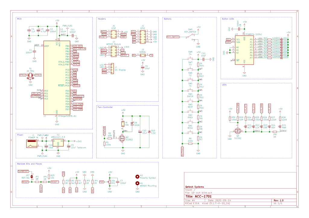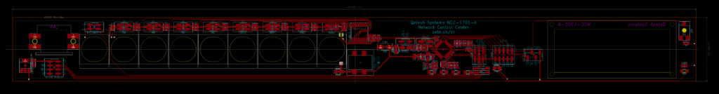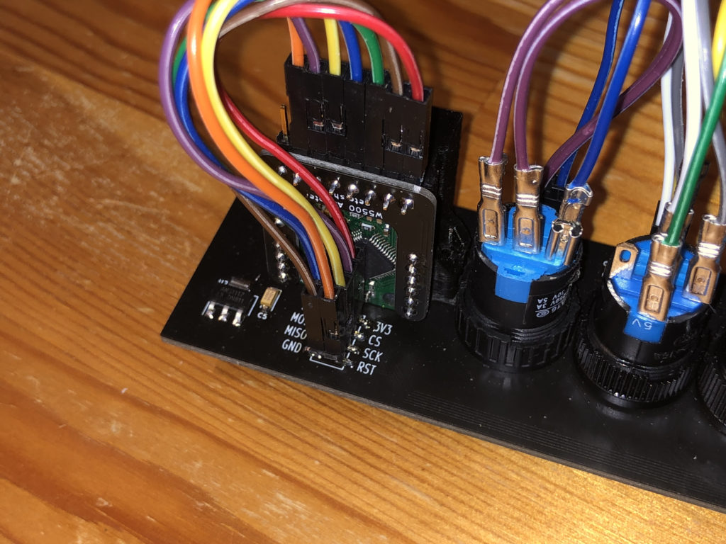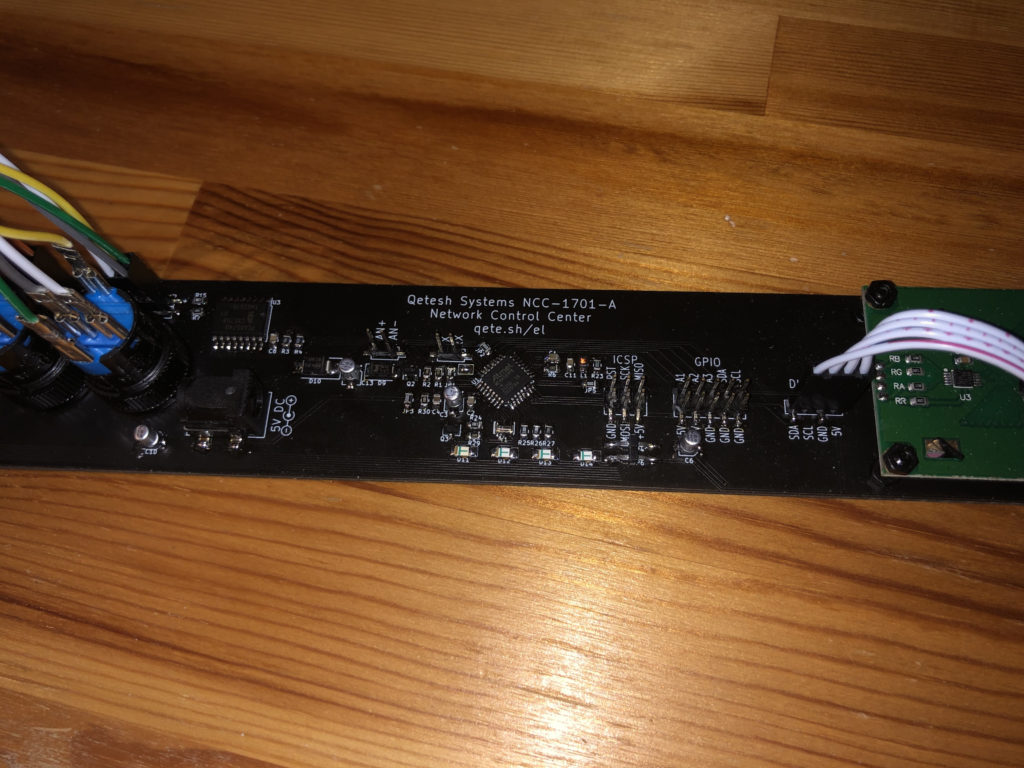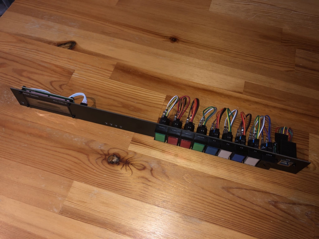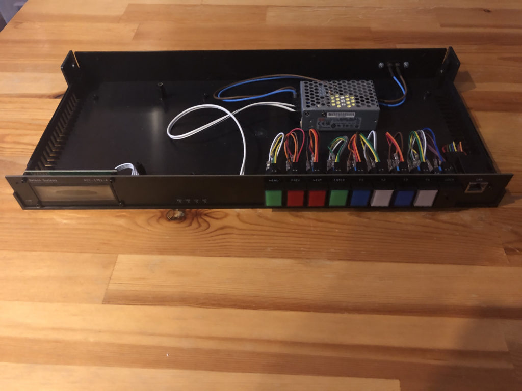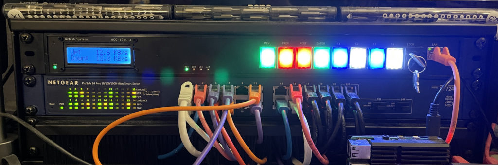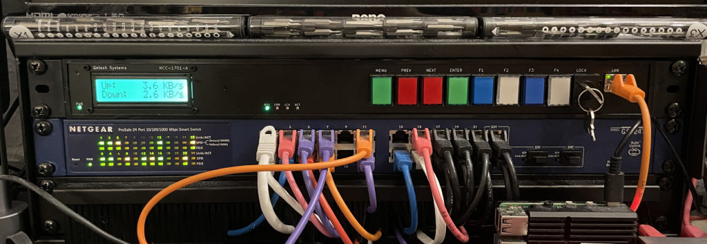
Another project in the category “Because I Can” – I had an unused, empty 19″ case for quite a while which needed a filling. After pondering different ways to create a nice looking front panel I got the idea to have a PCB produced for that. And since I didn’t want more than one board for this project, all components had to go on the back of that. This turned out to be a bigger challenge than anticipated since every via would be visible and I wanted a smooth surface. The only vias are hidden behind the buttons and on the edge of the board where the case is covering them. There isn’t a single trace on the front so routing everything was not as easy as usual. The device is controlled by an ATmega328PB, running at 20MHz. A PCA8574 is used to control the LEDs in the buttons. A W5500 module is used for Ethernet.
I can say this board is completely over-engineered for what it’s doing but it looks nice and that was its main purpose! In the end this was at least good practice for PCB design. I also learned a valuable lesson from this project: Triple check IC pins… the first version of the board had SCL and SDA of the PCA8574 swapped and I only noticed that after soldering everything in… But I still tested a lot with the first version before ordering new boards and changed quite a few things.
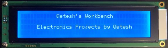
The first version had no PWM for the LEDs and they were way brighter than planned so that was added. Also version 1 had a 16 pin connector for the LCD, controlled by a second PCA8574 which was removed in favor of a display with direct I2C support (and RGB backlight!). The LEDs are special as in they are reverse mounted and the footprint for those also needed a few changes since the manufacturer (JLCPCB, not a sponsor!) wasn’t able to drill square shaped holes… I wonder why?! The potentionmeter, also reverse mounted, is left over from the original LCD but now got connected to an analog input to control the display brightness.